|
Design for
Manufacturing – Quick tables of Interconnection/Wire-bond
Basics
1. Electric Current vs. Wire Size
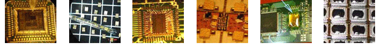
2. Basics of Board, Substrate, Package, Flex
3. Gold Plating
4. Trace Attributes
Layout
5. Bond-Pad size on Die vs. Wire Size
6. Die Mounting-Pad Size vs. Die Size
7. Better Trace Layout
8. Geometry re Trace-End
9. Obstacle Position, away from the 2nd bond-point
Process
10.
Assembly Process Concerns
11.
Eutectic Attach and Epoxy Attach
12.
Mistakes & Advice on Board Preparation
13.
Assembly Issues and Answers
14.
Bond Variables
15.
Wire-Bond Quality Data
16.
Glob Top Encapsulation
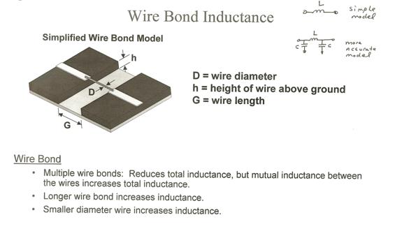
Advance concern: Wire Inductance
17.
Principles of Wire Parasitics
18.
Inductance of 2 Wires
19.
Wire Inductance Calculation, Simplified
20.
Wire Length for Inductance Concern
21. Wire Inductance
Table & Calculation, Realistic
1. Electric Current vs. Wire Size
|
Material
|
Wire dia,
mil
|
Max. Amp
|
|
Length < 40 mil
|
0.1” > Length > 40 mil
|
|
Gold
|
0.7
|
0.556
|
0.380
|
|
Gold
|
1.0
|
0.949
|
0.648
|
|
Alum
|
0.7
|
0.407
|
0.208
|
|
Alum
|
1.0
|
0.696
|
0.481
|
|
Alum
|
2.0
|
1.968
|
1.360
|
Calculation Info
|
Electrical
|
Alum
|
Gold
|
|
Specific Resistance, ρ
|
Ω
(mm
²)/ M
|
0.0278
|
0.0222
|
|
Specific conductance,
η = 1/ρ
|
M /
Ω (mm
²)
|
36
|
45
|
|
Maximum current in
DC amperes or rms AC ampers
I max = K d
³/²,
d =
wire dia. in
|
K
|
Length
< 40 mil
|
22,000
|
30,000
|
|
Length
> 40 mil
|
15,200
|
20,500
|
2. Basics of Board, Substrate, Package, Flex
|
|
Board,
FR-4 PCB
|
Substrate,
Thick Film
|
Packages,
Metal
|
Flex
|
|
Base Material
|
FR-4
(Epoxy)
|
Al2O3
(Ceramics)
|
Kovar,
Fe52Ni29Co18
|
Polyimide (Kapton);
Polyester (Mylar)
|
|
Conductor
|
Cu + Ni +
Au plating
|
Au, PdAg, PdPtAg, Cu
|
|
Cu + Ni +
Au plating
|
|
Dielectrics
|
Epoxy, FR-4
|
Glass-Ceramics
|
Glass-Ceramics
|
Kapton;
Mylar
|
|
Fabrication
Processes
|
Photolithography, etch, collate, sheets, laminate, Drill vias, plate
|
Sequentially print, dry, afire conductor, dielectric, and resistor pastes
|
machining
|
Photolithography, etch, collate, sheets, laminate, Drill vias, plate
|
|
Line width,
um, min
|
75
|
125
|
|
75
|
|
Via dia, um min
|
200
|
250
|
|
<200
|
|
Conductor Resistance, mW/sq
|
0.15~1
|
2-100
|
|
0.15~1
|
|
CTE (or TCE), ppm/8C
|
4~16
|
4~7.5
|
5.5
|
18
|
|
Thermal conductivity,
W/m@K
|
low
|
Much higher
|
16.5 W/m.C @25C;
17.6 W/m.C
@ 100C
|
low
|
|
Tolerance to temp extremes
|
Low
|
High
|
|
Low
|
|
Relative cost
|
Low
|
High
|
High
|
Low
|
3 Gold Plating
3.1 Over copper on Board, IPC-4552,
|
1st level
|
Ni
|
150 ~ 200 micro inches nickel over copper clad PCBs
|
|
2nd level
|
Au
|
5 ~ 15 micro inches malleable, 99.99% pure gold, over nickel.
|
3.2 Commercial Plastic Package, e.g. PBGA
|
1st level
|
Ni
|
50 micro inches min.
|
|
2nd level
|
Au
|
20 micro inches min.
|
3.3 Ceramic Package, e.g. Kyocera’s C-DIP
|
1st level
|
Ni
|
60 ~ 350 micro inches
|
|
2nd level
|
Au
|
60 ~ 225 micro inches
|
3.4 Substrate, Thick film
|
Au
|
400 micro inches, Stencil printed
|
4. Trace Attributes
|
Material
|
Die
Bondability
|
Wire
bondability
|
Solder-ability
|
Corrosion
resistance
|
|
Eutectic
|
Epoxy
|
Gold
|
Alum
|
|
Au
|
good
|
excellent
|
excellent
|
good
|
per solder type
|
excellent
|
|
PdAu
|
NG
(no good)
|
excellent
|
Fair
to poor
|
fair
|
good
|
excellent
|
|
PdAg
|
NG
|
excellent
|
good
|
good
|
good
|
good
|
|
PdPtAg
|
NG
|
excellent
|
good
|
good
|
good
|
good
|
|
Cu
|
NG
|
excellent
|
fair
|
fair
|
excellent
|
poor
|
|
Ni
|
NG
|
excellent
|
NG
|
good
|
NG
|
excellent
|
|
W
|
NG
|
excellent
|
NG
|
NG
|
NG
|
good
|
5. Bond-Pad size on Die vs. Wire Size
|
Pad Size,
mil x mil
|
Min.Pad-Pitch, mil
|
Wire dia, mil
|
|
Side
|
Corner
|
|
4 x 4
|
5
|
6
|
>=1.0
|
|
3 x3
|
4
|
5
|
1.0
|
|
2.6 x 3
|
3.5
|
4.5
|
1.0 or 0.7
|
|
2.0 x 2.4
|
2.5
|
3.5
|
0.7
|
6. Die-Mounting-Pad Size vs. Die Size
Die-mount-pad (A x B) vs. Die size (dl x w)
|
Comply with
MIL-STD-883
|
A x B > =
|
(dl + 8 x 2 mil) x (w + 8 x 2 mil)
|
|
Don’t care
MIL-STD-883
|
A x B =
|
dl x dw
|
7. Better Trace Layout
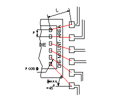
Trace-end Layout
|
Uniform & even
|
staggered
|
hoe
|
|
Better, if
|
They are parallel to
the bond-pad of each side of die
|
|
Use stagger way
to narrow the trace pitch
|
|
Apply the hoe shape
at the trace end
|
|
Avoid
|
To wire trace and die-pad in big angle,
e.g. corner wires and angle wires
|
Warning: The corner wires of wide angle might cause the electric
short on the chip surface.
8. Geometry re Trace-End
8.1 Trace-end Width
|
Min. width, mil
|
Comfort width, mil
|
|
2.6 ~ 3
(The flatness of
profile is difficult.)
|
5~8
|
8.2 Trace-end Position
|
Wire dia., mil
|
Distance away from
chip, mil
|
Comfortable distance
away from chip,
mil
|
|
Max.
|
Min.
|
|
Forward
Bonding
|
Reverse
Bonding
|
Level difference
(1st/2nd bond)
0 mil
|
Level difference
6 mil
|
Level
difference 11 mil
|
|
0.7
|
90
|
150
|
8
|
12
|
25
|
35 ~ 55
|
|
1
|
150
|
210
|
10
|
15
|
35
|
40 ~ 70
|
9. Obstacle Position, away from the 2nd bond-point
Minimum Obstacle Distance away from the 2nd
bond-point
 |
|
H, mil
|
W, mil
|
|
20
|
40
|
|
40
|
45
|
|
60
|
50
|
|
80
|
55
|
|
100
|
65
|
|
10. Assembly Process
Concerns
Remember these
|
Sequence
|
Go first with high temp process; then
follow with low temp process.
|
|
Avoid
|
“Piggyback” mounting
|
|
Use tin-lead solder and flux in hybrid circuit
that has wire-bond.
|
|
Have components on the back side of bond area before bonding.
|
|
Do wedge bond with Alum or Gold wire
|
It’s more tolerable to the variance of surface condition.
|
|
Require max. current
|
Bond two wires on pad instead of one, if pad is large, e.g. diode.
|
11. Eutectic attach and Epoxy attach
Comparison of Alloy
and Epoxy Attachment Methods
|
Eutectic/Alloy Attach
|
Epoxy Attach
|
|
Provide electrically conductive path
|
Can be electric conductive or insulative pending on epoxy used
|
|
High thermal conductivity
|
Low for insulative epoxy; better with silver-filled epoxy
|
|
High material cost
|
Low material cost
|
|
High temp process
|
Low temp process
|
|
No outgassing
|
Outgassing; requires vacuum control sometimes
|
|
Generally require fluxing and special cleaning
|
No flux required
|
|
Can be rigid and brittle, causing cracking of large die
|
Inherently flexible, provide stress
relief
|
|
No bleed-out
|
May bleed-out during cure
|
12. Mistakes & Advice On Board Preparation
12.1 Common
mistakes
|
|
Description
|
Potential trouble
|
Last solution if the
trouble happens
|
|
1
|
Form a big wire angle between the corner bond-pads & traces
|
Wire short on die surface
|
Offset die placement;
Use 0.7 mil wire
|
|
2
|
Limited gap between die & trace
|
Can’t form a wire loop
|
Use 0.7 mil wire
|
|
3
|
Small bond-pad pitch
|
Can’t bond with 1 mil;
Short on chip surface
|
Use 0.7 mil wire
|
|
4
|
Small bond-pad size
|
Oversize with 1 mil
|
Use 0.7 mil wire
|
12.2 All kinds of mistakes
|
|
Macro-checking
|
Microscopic Observation
|
Create troubles in
Percentage rate
|
Advice
|
|
1
|
Board is too thin
|
board warpage or camber
|
wire-bond non-stick
|
Thicker board
|
|
damping during bonding
|
|
2
|
Board size is too large
|
---
|
No flexibility of module(s)
|
Max < 3” ~4” Square;
Preferred, about 1.5” x 1”.
|
|
Circuit is too big and rigid
|
|
3
|
Bad trace quality
|
Bare copper surface
|
---
|
Wire-bond Non-stick
|
Gold/ Ni plated over
Copper
|
|
Oxidized surface
|
Scattered dark spots
or dark cloudy
|
|
Foreign matter
contamination
|
Oily or dull surface
|
|
Narrow trace
|
Cross-section is in round profile
rather than flat.
|
|
4
|
Die-mount-pad
|
Solder residue
|
Flux migrate and spread around
|
Wire-bond Non-stick
|
Don’t touch the die-mount -pad.
|
|
Large thru-holes in pad area
|
Force die-placement shifted from the
designed position
|
wire-bond difficulty in terms of
wire-length or corner wire bonding
|
Hole dia < 1/3 die width
|
|
5
|
Other components on board
|
Components are too high or too close
to the bond-area
|
wire-bond difficulty or impossible
|
Check with wire-bond specialist in-advance
|
|
6
|
Solder components on top surface
|
Chemical residue spread all over the
surface
|
Wire-bond
Non-stick
|
Use conductive epoxy
instead of soldering
|
|
7
|
Residue of solder flux, Chemical
cleaner, metal chips, foreign matters
|
Micro-particles or chemical
residue on surface
|
Wire-bond non-stick
|
Don’t do washing, flushing, wiping.
|
|
8
|
Mechanical polished (shiny) board
surface
|
Mountains and valleys surface with
dirt hide in grooves
|
Wire-bond non-stick
|
Should never do sanding, polishing.
|
|
9
|
Solder spots on back surface
|
Create minor gap between board and
work-holder
|
Clamping issue or even
wire-bond non-stick
|
Inform wire-bond specialist in-advance to modify the clamping fixture
|
|
Damping during bonding
|
|
10
|
Jumper wires on back surface
|
Create minor gap between board back
surface and work-holder
|
Clamping issue or even
wire-bond non-stick
|
Inform wire-bond specialist
in-advance to modify the clamping fixture.
Place jumper wires on top surface.
|
|
Damping during bonding
|
13. Assembly Issues and
Answers
Issues
Answers
|
1.
Epoxy Die-Attach
•
Many cavities show up
•
Hand touches units
during inspection
|
•
Cure epoxy in a higher temp, short time.
•
Design a mechanism that can let you take units out easily.
•
Design a carrier.
|
|
2.
Epoxy seal, e.g. lid-attach, RingFrame-attach
•
Bad appearance and low thru-put
|
•
Design the process fixtures.
•
Improve programming.
|
|
3.
Eutectic Die-Attach
•
Can’t hold the substrate.
•
Keep raising the temp setting.
|
•
Source work-holder from Internet.
•
Design the fixture.
•
Improve the work-holder surface.
|
|
4.
Solder Attach, Lead-frame, < 40 Leads
•
Bad solder joints or low thru-put.
•
Ineffective cleaning
|
•
Develop process tools or manual machine.
•
Choose a solder paste of water soluble flux.
•
Develop the process tools.
•
Use DI water.
|
|
5.
Hermetic seal, with furnace.
•
Failed at visual inspection or
bubble
test.
|
•
Control the clamping force with gram gage.
•
Improve the thermal flow of vehicle.
•
Tune the temp profile.
|
|
6.
Wedge bond
•
Non-stick
•
Break at heel
•
Bad bond accuracy.
•
Cratering
|
•
Tune the bond parameters. See Graphics A&B.
•
Tighten the bonding wedge.
•
Improve substrate clamping.
•
Clean material surface. See Graphics A&B.
•
Choose a different wedge.
•
Low the power. See Graphics A&B.
•
Minimize the back bend of looping.
•
Improve programming, machine calibration.
•
Lower the power. See Graphics A&B.
•
Adjust the approaching speed.
See Graphics
A&B.
•
Improve clamping.
|
|
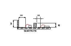
7.
Ball bond
•
Ball bond size is larger.
•
Weak transition from the stitch bond to the wire.
|
•
Reduced Free-Air-Ball size or shorten the distance between wand and
capillary.
•
Improve wand mechanism.
•
Choose a different capillary.
•
Lower the bond force.
|
14.
Bond
Variables
|
|
Ball bond
|
Wedge bond
|
|
Welding parameters
|
Power, Force, Time, EFO,
Temperature,
|
Power, Force, Time, Temperature
|
|
Looping parameters
|
Wire length,
|
Wire Clamp open/close position
|
|
Elevation between bonds
|
Forward bond, reverse bond
|
|
Wire straightness, sagging
|
Wire length, elevation, straightness, sagging
|
|
Other parameters
|
Crescent of 2nd bond:
Capillary cone formation, bond force
|
Tail at 1st bond:
Wire break & feed of wire-clamp
|
|
Free Ball Size: Wand flame off power, time, swing repeatability,
|
|
15. Wire-Bond Quality
Data
15.1 Pull Test, Per MIL-STD-883
|
Non-Destructive
Pull Test.
(some % of wire quantity)
|
Wire size, mil
|
Alum,
Gram force
|
Gold,
Gram force
|
|
0.7
|
1.2
|
1.6
|
|
1.0
|
2.0
|
2.4
|
|
Destructive Pull Test.
(Wires are on coupons)
|
0.7
|
1.5 min.
|
2.5 min.
|
|
1.0
|
2.5 min.
|
3.0 min.
|
15.2
Bond Deformation, per MIL-STD-883
|
|
No device shall be acceptable that exhibits
|
|
Inspect
|
Ball bond
|
Wedge bond
|
|
bonds on die, substrate or package post
|
Method 2017.6
3.1.4.1. a
… the ball bond diameter is less than 2.0 time or
greater than 5.0 times
the wire diameter
|
Method 2017.6
3.1.4.2.a Re: Alum wire
… less than 1.2 times or greater than 2.5 times the wire diameter in width,
or less than 1.5 times or greater than 5.0 times the wire diameter in length
3.1.4.2.b Re: Gold wire
… less than 1.5 times or greater than 3.0 times the wire diameter in width,
or less than 1.5 times or greater than 5.0 times the wire diameter in length
3.1.4.4.g Re: tail
exceed 2 wire diameters in length at
bonding pad or
4 wire diameters in length at the package post or
10 mils
|
16. Glob Top Encapsulation
|
Epoxy,
Loctite
|
Glob top
|
Application
|
|
shape
|
size in
terms of
Wire-bond
area (L x W)
|
|
#349
|
High
viscosity
|
Round
dome
|
L + 30
mil x 2;
W+ 30 mil
x 2
|
Where
total thickness is
Not a
concern
|
|
#363
|
Low
viscosity
|
Odd dome
or “X”
shaped dome
|
L + 80
mil x 2;
W+ 80 mil
x 2
|
Where
total thickness is
demanded
as low as possible (<20 mil)
|
17. Principles of Wire Inductance
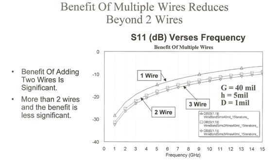
18. Inductance of 2 wires
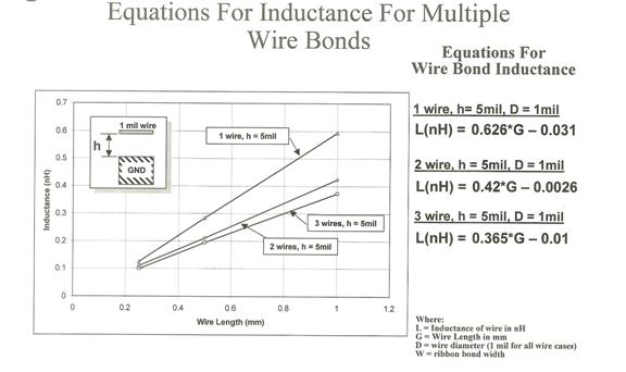
19. Wire Inductance Calculation,
Simplified
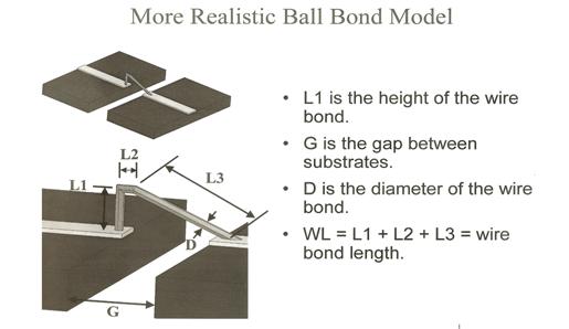
20. Wire Length for Inductance
Concern
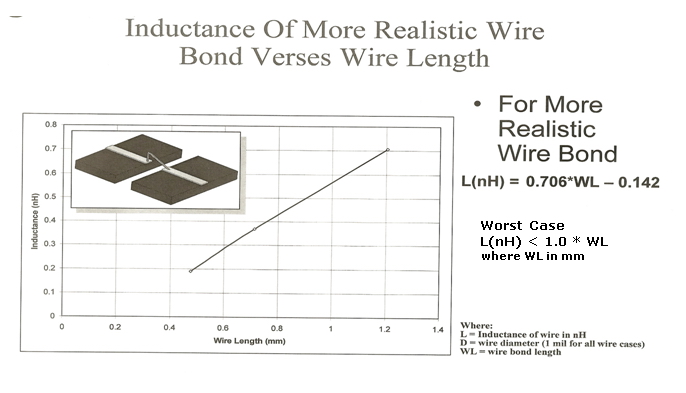
21. Wire Inductance Table &
Calculation, Realistic
|